
The Latest Innovations in PCB Design and Development
Printed circuit boards are a growing industry around the world. Read through this list of the latest innovations in PCB design and development to know about.
Sometimes, change is resemblant to what Dorothy remarks in The Wizard of Oz: “Toto, I have a feeling we’re not in Kansas anymore.” Have you seen the changes happening in our world lately? Newfangled standards are set in the consumer marketplace on the daily. The PCB design and manufacturing field is one such optimized area changing to fit the lifestyles of modern society.
The rising wave of innovative technology has pressed electrical engineers and designers to adapt printed circuit boards designs to the digital era. How much do you know about this pivotal and impressive industry? Let’s take a closer look at the latest innovations in PCB design and development.
The IoT: Extreme Customizability for Devices
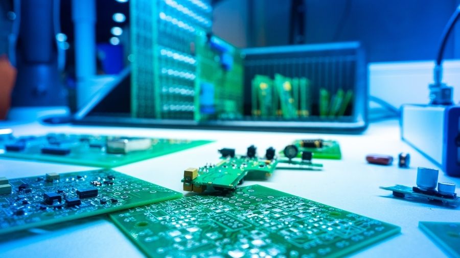
Printed circuit boards are the core of today’s most utilized electronic devices, no matter how simple or complex they may be. These days, the Internet of Things (IoT) continues to significantly change PCB design and incentivize the building of boards on a smaller scale. Design software is paving the way to create customized PCBs that fit within unique and advanced devices.
IoT devices are a network of physical objects embedded with technology to connect and exchange data over the Internet. PCB designers must make the most out of the available space on the board with IoT components, pushing the possibilities of technology to its limits for functionality.
Sensor Technology: Cameras and Wearables
Speaking of advanced software, another of the latest innovations in PCB design and development is board cameras. Some of the most sophisticated products on the market are powerful because of their embedded sensor cameras attached directly to a PCB. Because of their small size, current cameras are relatively simple with a lens, aperture, and image sensor. That is bound to change.
The high development rate of PCB cameras provides a clear picture of the future—for uses beyond mere smartphones. As a matter of fact, their use within medical instruments already helps save lives. Physicians can examine the body with capsule devices without the need for invasive surgery. Surveillance technology also benefits from board cameras to ensure security within critical facilities or environments. The best part is that mega-pixelization and clarity continually get better and better.
3D Printing Technology: Assembly Error Correction
You’ve surely heard about this rising technology over the last decade: 3D printing. How does this development influence PCB design? Generally speaking, functional PCB design for beginners is no simple feat. The intricacies of design may prove difficult to translate during component layering and manufacturing. This is where 3D-printed electronics may come into play.
Fully functional 3D printers could overcome common PCB design. This type of technology has yet to be embraced and adopted on a mass scale, but there’s no questioning the endless possibilities for the future. As the market develops new technologies to meet high demands, keep this background knowledge of PCBs in mind. Improved PCB design is the answer to life-changing consumer electronics.


%20(1).png)


.png)

.png)
.png)


0 Comments